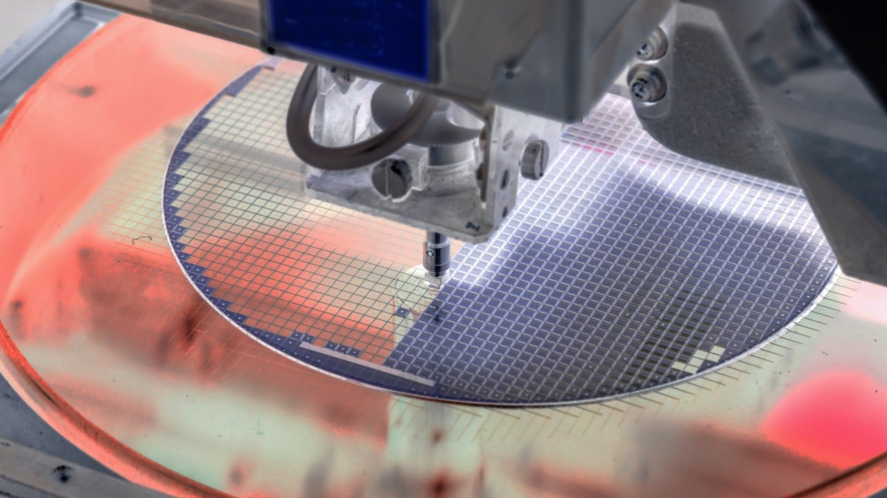
For years, the playbook for domestic memory manufacturers in China looked remarkably uniform: scale up standard fabrication lines, absorb steep yield penalties, and capture low-margin volume in consumer electronics before foreign export curbs could tighten further. That baseline survival strategy has run its course. With artificial intelligence hardware workloads and high-density servers rewriting the economics of computation, raw wafer fabrication is no longer the primary bottleneck for domestic memory producers. The real contest has shifted upward, away from the silicon cleanroom floor and directly into the back-end assembly line.
Major domestic players like ChangXin Memory Technologies and Yangtze Memory Technologies are pouring billions into advanced packaging architectures, chasing a transition from commodity volume providers to high-value system builders. This pivot is not merely a corporate upgrade; it is an urgent structural response to severe trade restrictions on extreme ultraviolet lithography and front-end tooling. When you cannot shrink lithography nodes below specific thresholds using standard machinery, you stack vertically. You rely on through-silicon vias, hybrid bonding, and 2.5D integration to squeeze more performance out of older, wider transistor geometries.
Understanding this shift requires looking closely at how memory dies actually interface with processors in modern data centers. In a conventional server architecture, a DRAM chip sits on a printed circuit board a few inches away from the central processor, linked by copper traces that introduce latency and power loss. In high-performance computing clusters running large language models, that distance creates a fatal data bottleneck. The processor starves for lack of input, waiting milliseconds that stretch into eternities in machine-learning terms.
To solve this, global memory leaders turned to High Bandwidth Memory, stacking multiple DRAM dice vertically and stitching them directly to a logic processor using microscopic silicon pillars called through-silicon vias. For domestic storage firms, mastering this vertical architecture is an existential necessity. Without high-end packaging capabilities, any memory chip produced on a constrained fabrication node remains locked out of the lucrative AI accelerator ecosystem. Engineers can manufacture millions of standard wafers, but if those wafers cannot be densely interconnected via advanced substrates, they are structurally obsolete for modern data center deployments.
The capital expenditure figures tell the story with brutal clarity. Specialized domestic OSAT providers alongside dedicated memory designers are aggressively expanding facility footprints to handle high-density stacking. Tens of billions of yuan are flowing into regional packaging hubs, turning test-and-assembly floors into the most critical battlegrounds in the domestic semiconductor supply chain.
Yet this transition faces severe hurdles that corporate press releases rarely acknowledge. Front-end lithography may grab headlines, but advanced packaging is an exacting metallurgical and mechanical discipline. Consider a hypothetical scenario involving an eight-layer DRAM stack bonded to an application processor. If the thermal expansion coefficients of the underlying silicon substrate, the copper micro-bumps, and the encapsulation molding compounds do not match precisely, microscopic warping occurs under thermal stress. A single warped connection across thousands of through-silicon vias ruins the entire stack during the final bake cycle.
Achieving acceptable yields at scale requires specialized bonding tools, precision dicing saws, and specialized carrier wafers that remain heavily restricted by international trade enforcement. While firms have made notable strides delivering engineering samples to domestic system integrators, transitioning from a successful lab sample to a commercially viable volume product involves a brutal valley of death. Customer qualification cycles for enterprise-grade memory take years, not months, because data center operators cannot risk catastrophic field failures over minor cost savings.
Furthermore, a quiet convergence is underway between traditionally segregated product categories. Historically, the domestic memory sector operated with a strict division of labor: one major firm focused almost exclusively on dynamic random-access memory, while another specialized in three-dimensional NAND flash storage. That clean separation is dissolving. Pressured by shifting domestic demand and the need to offer complete system bundles to local original equipment manufacturers, these giants are expanding into each other's historical territories.
This cross-encroachment means that packaging lines must now be versatile enough to handle both volatile memory dies and non-volatile flash arrays under unified architectures. It introduces fresh engineering friction. Flash memory and high-speed DRAM have vastly different thermal profiles, refresh rates, and power delivery requirements. Packaging them into unified multi-chip modules demands sophisticated substrate design that bypasses traditional packaging conventions entirely.
The geopolitical dimension adds another layer of friction to this climb up the value chain. Global equipment vendors based in the United States, Europe, and Japan supply the precision dispensing, laser trimming, and inspection tools required for advanced back-end work. As export controls tighten around assembly machinery alongside lithography, domestic equipment developers are racing to fill the void. Firms specializing in pick-and-place robotics and advanced metrology are seeing unprecedented demand to replace foreign lines. Some of these domestic tools perform admirably in controlled environments, but matching the throughput and uptime of legacy international machinery remains an uphill battle on factory floors running twenty-four hours a day.
The ultimate test for these packaging initiatives will not be whether they can produce impressive demonstration units for trade delegations or financial markets. It will be whether they can supply domestic tech giants with enough reliable, high-density memory to sustain local cloud infrastructure without relying on imported components. If they succeed, the center of gravity for packaging innovation will permanently decentralize. If they stumble, the climb up the value chain will stall at the threshold of mass production.